Their gamble however is that they need to figure out DSA, a long storied technology that uses self-forming polymers to allow less light to sharply etch smaller features.
If they figure out DSA, they will likely be ahead of TSMC. If not, it will just be more very expensive languishing.
This is the industry roadmap from 2022: https://irds.ieee.org/images/files/pdf/2022/2022IRDS_Litho.p... If you look at page 6 there is a nice table that kind of explains it.
Certain feature sizes have hit a point of diminishing returns, so they are finding new ways to increase performance. Each generation is better than the last but we have moved beyond simple shrinkage.
Comparing Intel’s 14A label to TSMCs 16A is meaningless without performance benchmarks. They are both just marketing terms. Like the Intel/AMD CPU wars. You can’t say one is better because the label says it’s faster. There’s so much other stuff to consider.
Very interesting document - lots of numbers in there for real feature sizes that I had not seen before (Table LITH-1).
And this snippet was particularly striking:
Chip making in Taiwan already uses as much as 10% of the island’s electricity.
If Intel pulls off DSA, they will be using a newer generation of technology compared to TSMC using an optimized older generation. Could TSMC still make better chips? Maybe. But Intel will likely be better.
Dsa is one of many patterning assist technologies, just...an old one. Neat, but not 'new'. You use patterning assist to make smaller, more regular features, which is exactly what the 16a vs 18a refers to.
That has somewhat less to do with performance, which is tied as much to material, stress, and interface parameters. Nothing gets better from being smaller in the post dennard scaling era, the work of integration is making better devices anyway.
Patterning choices imply different consequences. For example,.a.double euv integration can take advantage of spacer assists to reduce ler and actually improve cdu even with a double expose. Selective etch can improve bias, spacer trickery can create uniquely small regular features that cannot be done with single patterns. Conversely, overlay trees get bushier, and via CD variance can cause horrific electrical variance. It is complicated, history dependent, and everything is on the developmental edge.
To the best of my knowledge, DSA never made it out of the lab.
Is Intel working on "an optimized older generation" as a backup plan? I don't follow semiconductors very closely, but my impression is the reason they're "behind" is they bet aggressively on an advanced technology that didn't pan out.
If that's the actual root cause, then Intel's lagging is due to optimizing their balance sheets (investors like low capital expenditures) at the expense of their technology dominance.
Earlier it was AMD. The most prominent era since their Athlon XP CPUs turned out to be noticeably more performant per GHz than Intel in 2001.
It is my understanding that only ASML had cracked the EUV litography, but if there's another company out there, that would be an interesting development to watch.
Ackshually, EUV was cracked by Sandia Labs research in the US, with EUV light sources built by Cymer in the US. ASML was the only one allowed to license the tech and integrate it into their steppers after they bough Cymer in 2013. Hence why US has veto rights to whom Dutch based ASML can sell their EUV steppers to, as in not to China, despite ow much ASML shareholders would like that extra Chinese money.
More like it was started. There were a ton of gnarly problems left that took over ten years and billions of € to solve.
Producing a few flashes of EUV and getting a few photons on the target is relatively easy. Producing a lot of EUV for a long time and getting a significant fraction (...like 1%) of the photons on the target is very hard.
https://www.asml.com/en/news/stories/2022/making-euv-lab-to-...
There's no such thing in capitalism. Limited supply semi is(was) a bidding war, where China had a blank cheque and was willing to outbid everyone else to secure semi manufacturing supremacy.
Do you think Intel or TSMC could have scored all that ASML supply at that price if China would have been allowed to bid as well? ASML would have been able to score way higher market prices per EUV stepper had China been allowed in the game, and therefore higher profits.
You think ASML shareholders hate higher profits or what? Nvidia sure didn't during the pandemic. You wanted a GPU? Great, it would cost you now 2x-3x the original MSRP because free market capitalism and the laws of supply and demand.
ps. Intel used to own 15% of ASML in 2012, now they own less than 2%.
And, to think, it's all done with light !
We live in interesting times !
230 M/mm2 translates to 33nm "half-pitch".
Of course, transistors aren't square and aren't so densely packed, but these numbers are more real IMO.
Gallons per mile only makes sense when you are talking about dragsters.
incidentally, this is the measure rest of the world is advertising, except usually in liters per 100km.
there's a good reason for this: comparisons linear instead of inversely proportional. 6l/100km is 50% better than 9l/100km. 30mpg vs 20mpg is... not as simple.
How so?
I guess it's a matter of approach. Europeans are traveling familiar, constant distances and worry about fuel cost. Americans just fill up their tank and worry how far they can go :)
"Quick, which is better: Replacing an 18-mpg car with a 28-mpg one, or going from a 34-mpg car to one that returns 50 mpg? Researchers at Duke University say that drivers find it easier to select the right answer when efficiency is expressed as gallons per 100 miles (g/100m).
So 18 mpg (or 5.5 g/100m) versus 28 mpg (3.6 g/100m)--an increase of 10 mpg--represents a 52 percent reduction in consumption.
If you trade in a car rated at 34 mpg for one rated at 50 mpg, its a 16-mpg improvement, so we ought to see those gas card bills plummeting, right? Actually, after a minute's worth of math, you'll get 2.9g/100m in the 34-mpg car and 2g/100m in the 50-mpg car--only half as big a gain as the original scenario. "
If you think of an SOC, the chip in your phone, more and more of the real estate is being dedicated to specialized compute (AI accelerators, GPUs, etc. vs general purpose compute (CPU).
At the enterprise scale, one of the big arguments NVIDIA has been making, beyond their value in the AI market, has been the value of moving massive, resource intense workloads from CPU to more specialized GPU acceleration. In return for the investment to move their workload, customers can get a massive increase in performance per watt/dollar.
There are some other factors at play in that example, and it may not always be true that the transistors/mm^2 is always lower, but I think it illustrates the overall point.
Basically, every single credit card sized security chip (including actual credit cards, of course) is a small processor running Java applets. Pretty much everyone has one or more in their wallet. I'd assume those were actual Java CPUs directly executing bytecode?
Not sure: https://en.wikipedia.org/wiki/Java_processor doesn't seem to mention any in current use. I am ignorant of the actual correct answer: I had simply presumed it is simpler to write the virtual machine using a commercial ISA than to develop a custom ISA.
Java Card bytecode run by the Java Card Virtual Machine is a functional subset of Java 2 bytecode run by a standard Java Virtual Machine but with a different encoding to optimize for size.
Patriot Scientific's Ignite processor family https://www.cpushack.com/2013/03/02/chuck-moore-part-2-from-...
ARM Jazelle technology https://developer.arm.com/documentation/ddi0222/b/introducti...
https://www.eetimes.com/nazomi-offers-plug-in-java-accelerat...
It's all dot-com era stuff and Sun Microsystems also created a Java OS that could run directly on hardware without a host operating system.
That's about it
Not to say that improvements and doing more with less are impossible, they probably aren't, but it's going to require significant per design human effort to do that.
There are the really obvious ones like on-board GPUs and AI accelerators, but even within the CPU you have optimizations that apply to specific kinds of workloads like specialized instructions for video encode/decode.
The main "issue", such as it is, is that this setup advantages vertically integrated players - the ones who can release software quickly to use these optimizations, or even going as far as to build specific new features on top of these optimizations.
For more open platforms you have a chicken-and-egg problem. Chip designers have little incentive to dedicate valuable and finite transistors to specialized computations if the software market in general hasn't shown an interest. Even after these optimizations/specialized hardware have been released, software makers often are slow in adopting them, resulting in consumers not seeing the benefit for a long time.
See for example the many years it took for Microsoft to even accelerate the rendering of Windows' core UI with the GPU.
Would it be that x2 (for front & back)?
E.g., 230 on front side and another 230 on back side = 460 MTr/mm2 TOTAL
Gotta love how we now have fractions of a near meaningless metric.
What more do you want? It’s as meaningful as a single number ever could be.
If you’re a consumer - if you don’t design chips - lower number means there’s some improvement somewhere. That’s all you need to know. It’s like horse powers on a car. The number doesn’t tell you everything about the performance under all conditions but it gives a rough idea comparatively speaking.
If you’re a chip designer then you never cared about the number they used in naming the process anyway. You would dig into the specification and design rules from the fab to understand the process. The “nm” number might show up in the design rules somewhere.. but that’s never been relevant to anyone, ever.
I really don’t understand why so many commenters feel the need to point out that “nm” doesn’t refer to a physical dimension. Who cares? It doesn’t have any impact on anyone. It’s very mildly interesting at best. It’s a near meaningless comment.
That's just patently wrong.
The measurement used to refer to feature size [0]. It used to be a physical measurement of a thing in nanometers hence nm
Now it's a free for all marketing team names it whatever the fuck they want. That's why you get stuff like intel 10nm being equivalent to AMD 7nm. [1]. It's not real.
>Who cares?
You...else we wouldn't be having this discussion
[0] https://en.wikipedia.org/wiki/Semiconductor_device_fabricati...
[1] https://www.pcgamer.com/chipmaking-process-node-naming-lmc-p...
trying to understand the economic impact of these announcements as I don't understand this topic well enough
This means that when different manufacturers use a different transistor design, their 'nm' process could be the same but their transistor density different.
The nm has always been a very rough approximate proxy for transistor density. Nothing has really changed about how what the number implies.
I find it so weird how so many people on hacker is so hung up on the “nm” numbering. None of these people are designing standard cell libraries and those that actually design standard cell libraries never cared about what’s in the marketing material anyway.
Lowe number means higher transistor density in some ways, on some parts of the chip. That’s all
We could just divide total gates by surface area for the chip, but that would confuse the process efficiency with the implementation details and then we sacrifice instructions per second for a marketing number.
mm² is perfectly adequate for what we are after.
"how large a planar FET should be for the transistor density used in this process"
Is this the case, I'm not entirely sure. If it is, there be a better unit for this measurement, absolutely.
PLANETS: PLANar Equivalent Transistor Size
Or hire a marketing team to figure a good one.
It's the same situation as when AMD started putting numbers in their Athlon XP SKUs to tell "this CPU performs just as good as intel of that frequency".
I, for one, think it makes sense. Because as I consumer I don't care about actual transited length or density, all I care about is: performance, efficiency, price. I can assume that going from TSMC N5 to TSMC N3 would result in an increase in efficiency and performance.
People that do care about those things (i.e. electrical engineers) most likely don't use marketing materials...
http://dataphys.org/list/grace-hopper-nanoseconds/
and the field of play here isn't 1D linear .. it's somewhere sort of a bit slightly > 2D (elements can be stacked, there are limitations on how much and how close)
Time to kick an ants nest here...
Quantum mechanics is a useless study that had no business being a scientific field. The most fundamental principles, like quantum superposition, can never be tested or validated and therefore could never be used to be predictive of anything other than similarly theoretical ideas.
It used to be the actual feature size which was quadratically proportional to transistor density.
Once feature size stopped being meaningful they continued using it by extrapolating from transistor density, ie whenever they would quadruple density they'd half this massive number. This, therefore, includes innovations like finfets and other " 2.5D" technologies
Is that largely correct? Because it's gross.
Just because you can't point to a specific feature and say that is 1.6nm, doesn't make the label meaningless as so many try to assert. It is a label that represents a process that results in a specific transistor density. What label would you prefer?
From roughly the 1960s through the end of the 1990s, the number meant printed gate lengths or half-pitch (which were identical).
At some point, companies started using "equivalences" which became increasingly detached from reality. If my 50nm node had better performance than your 30nm node because I have FinFETs or SOI or whatever, shouldn't I call mine 30nm? But at that point, if you have something less than 30nm somewhere in your process, shouldn't you call it 20nm? And so the numbers detached from reality.
So now when you see a 1.6nm process, it's think "1.6nm class", rather than that corresponding to any specific feature size, and furthermore, understand that companies invent class number exaggerations differently. For example, an Intel 10nm roughly corresponds to Samsung / TSMC 7nm (and all would probably be around 15-30nm before equivalences).
That should give you enough for a web search if you want all the dirty details.
Chip frequencies stagnated (end of Dennard scaling if I remember correctly) giving the impression that single threaded performance had stagnated, but since then chip makers have used increasing data and instruction parallelism to squeeze even more apparent single threaded performance out of chips. A 3ghz chip today is usually way faster on average code than a 3ghz chip 15 years ago. They also started expanding into multiple cores and adding more cache of course.
For fab processes we should just switch to transistor density. That still wouldn't capture everything (e.g. power efficiency) but would be a lot better than not-actually-nanometers.
For performance we really don't have a good single metric anymore since all these performance hacks mean different levels of gain on different code.
Indeed
May I propose transistor density divided by the (ergodic) average transistor switching power?
Not really the same thing, though. If I buy a chip that's advertised as 3.4GHz, it'll run at 3.4GHz. Maybe not all the time, but it'll achieve that speed. If I buy a chip advertised as being produced with a 3nm process, there's nothing even resembling 3nm on there.
The marketing departments of silicon companies are saving that as their ultimate weapon.
N1.6 is much better for naming node processes. Or even TSMC16.
They could invent codenames, or start using a better (physical) metric, if this one is no longer relevant.
[0] https://www.tomshardware.com/tech-industry/manufacturing/int...
The link you give doesn't have any details of Intel's 18A process, including no indication of it innovating in any way, as opposed to TSMC with their "backside power delivery" which is going to be critical for power-hungry SOTA AI chips.
Not saying TSMC won't, but they have so much more experience in the cutting edge.
https://www.intel.com/content/www/us/en/newsroom/news/powerv...
"Well, yes, we're behind TSMC in technology, but in our dreams we're way ahead!"
Getting these machines built and online is more important than what one machine (that might be less than 6 per year) can do.
The information, I'm sure, is buried in their papers, but I want to know what node processes are in products available now.
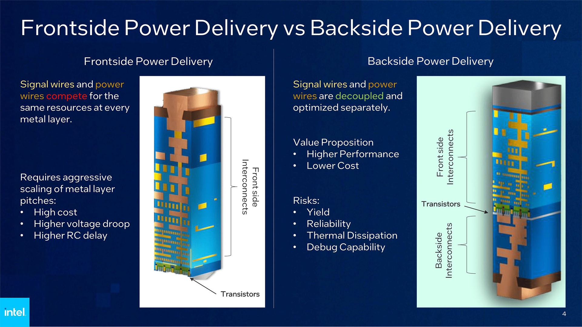
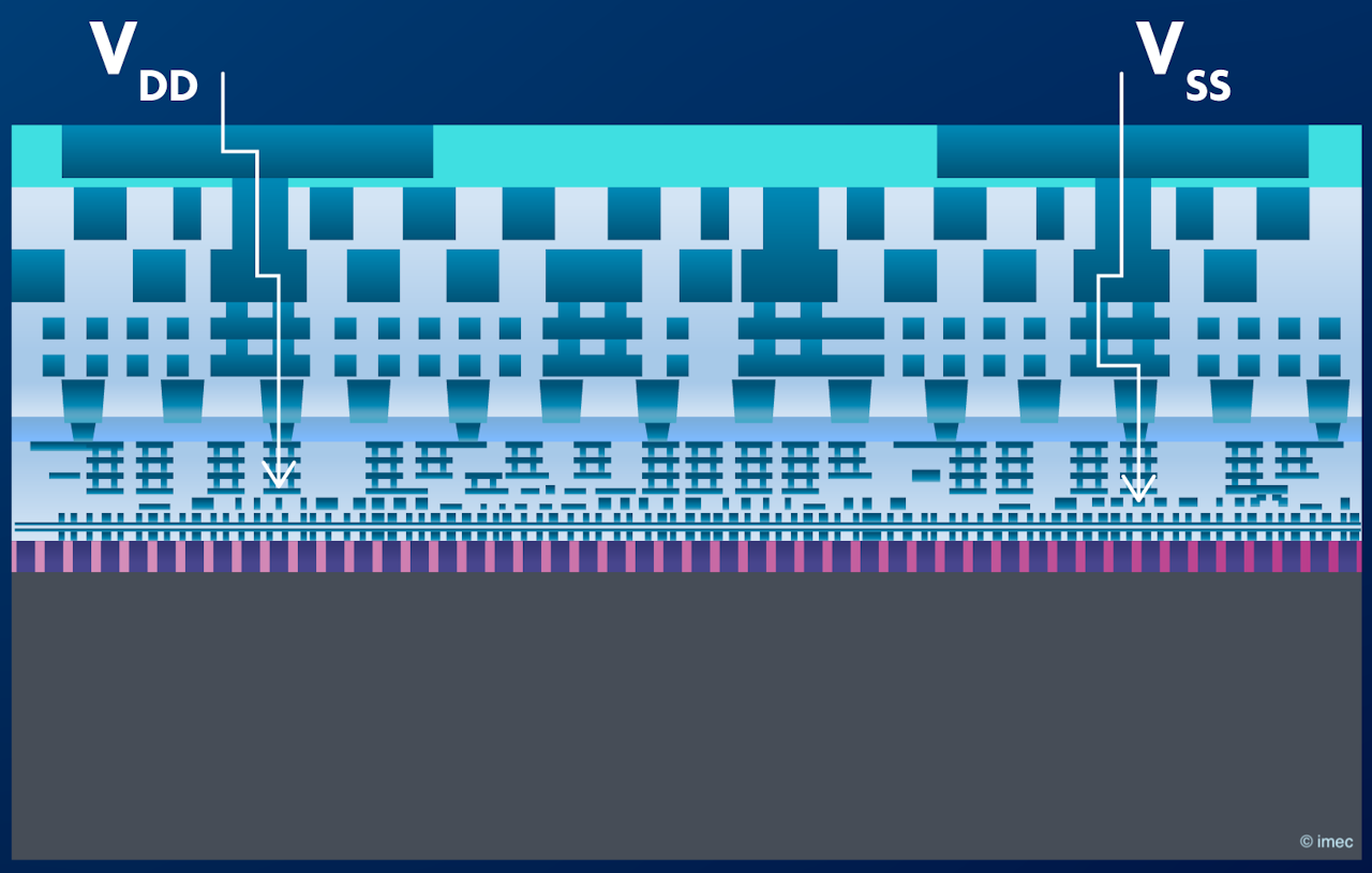
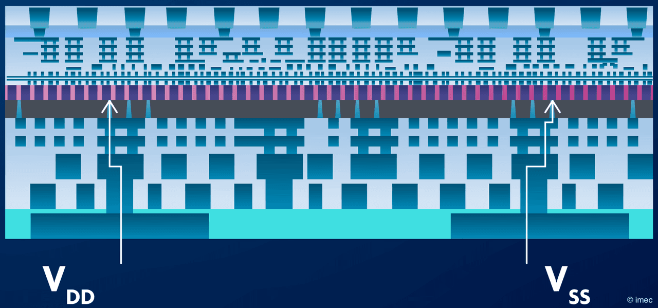
ICs are manufactured on silicon disks called wafers. Discs have two sides, and traditionally, everything was done on top. We can now do power on the bottom. This makes things go faster and use less power:
* Power wires are big (and can be a bit crude). The bigger the better. Signal wires are small and precise. Smaller is generally better.
* Big wires, if near signal wires, can interfere with them working optimally (called "capacitance").
* Capacitance can slow down signals on the fine signal wires.
* Capacitance also increases power usage when ones become zeros and vice-versa on signal wires.
* Big wires also take up a lot of space.
* Putting them on the back of the wafer means that things can go faster and use less power, since you don't have big power wires near your fine signal wires.
* Putting them in back leaves a lot more space for things in front.
* Capacitance between power wires (which don't carry signal) actually helps deliver cleaner power too, which is a free bonus!
This is hard to do, since it means somehow routing power through the wafer. That's why we didn't do this before. You need very tiny wires through very tiny holes in locations very precisely aligned on both sides. Aligning things on the scale of nanometers is very, very hard.
How did I do?
However, something like an 80286 didn't even require a heatsink, while my 80486 had a dinky heat sink similar to what you might find on a modern motherboard chipset. At the same time, on a micron node, wires were huge. A few special cases aside (DEC Alpha comes to mind), power distribution didn't require anything special beyond what you'd see on your signal wires, and wasn't a major part of the interconnect space.
Mapping out to 2024:
1) Signal wires became smaller than ever.
2) Power density is higher than ever, requiring bigger power wires.
So there is a growing disparity between the needs of the two.
At the same time, there is continued progress in figuring out how to make through-wafer vias more practical (see https://en.wikipedia.org/wiki/Three-dimensional_integrated_c...).
I suspect in 2000, this would have been basically restricted to $$$$ military-grade special processes and similar types of very expensive applications. In 2024, this can be practically done for consumer devices. As costs go down, and utility goes up, at some point, the two cross, leading to practical devices.
I suspect a lot of this is driven by progress in imagers. There, the gains are huge. You want a top wafer which is as close as possible to 100% sensor, but you need non-sensor area if you want any kind of realtime processing, full frame readout (e.g. avoiding rolling shutter), or rapid readout (e.g. high framerate). The first time I saw 3D IC technology in mainstream consumer use were prosumer-/professional-grade Sony cameras.
I have strong fundamentals, but again, I stopped following this closely maybe 15 years ago, so much of the above is speculative.
"Better" is relative, the layout introduces more fabrication steps so it's only better if you actually get some benefit from it. Decades ago designs didn't require as much power or have as many transistors to wire so it wasn't an issue.
You might as well ask why, since we can do it now, Shockley didn't simply start at 3nm. It's all a very long road of individual process techniques.
> You need very tiny wires through very tiny holes in locations very precisely aligned on both sides.
Key word here is "both sides". It has challenges similar to solder reflow on double sided boards: you need to ensure that work done on the first side isn't ruined/ruining work on the second side.
https://semiwiki.com/semiconductor-services/techinsights/288... seems to be a good description.
"The challenges with BPR are that you need a low resistance and reliable metal line that does not contaminate the Front End Of Line (FEOL). BPR is inserted early in the process flow and must stand up to all the heat of the device formation steps."
Contamination = metals used musn't "poison" the front-side chemistry. So they end up using tungsten rather than the more usual aluminium. (Copper is forbidden for similar chemistry reasons)
It also (obviously) adds a bunch of processing steps, each of which adds to the cost, more so than putting the rails on the front side.
Do you need to align that precisely? Can't the power side have very large landing pads for the wires from the signal side to make it much easier?
Historically, everything was etched, grown, deposited, and sputtered on one side of the wafer. The rest of the wafer was mostly mechanical support. The other side of the wafer is a universe away.
The world is more complex today, but that's a good model to keep in mind.
For a 3d integrated circuit, you would do this, and then e.g. grind away the whole wafer, and be left with a few micron thick sheet of just the electronics, which you'd mechanically place on top of another similar sheet. That's every bit as complex as it sounds. That's why this was restricted to very high-end applications.
As for whether the wafer is a huge ground plane, that's complex too, since it depends on the top of the device and the IC:
* First, it's worth remembering a pure silicon crystal is an insulator. It's only when you dope it that it becomes a conductor. The wafer starts out undoped.
* Early ICs had the whole wafer doped, and the collector of all the NPN transistors was just the wafer. There, it was a ground plane.
* SOI processes deposit a layer of glass on top of the wafer, and everything else on the glass. There, the wafer is insulated from the circuit.
So all of this can very quickly go in many directions, depending on generation of technology and application.
I'm not sure this post is helpful, since it's a lot of complexity in an ELI5, so I'll do a TL;DR: It's complicated. (or: Ask your dad)
Even so, I oversimplified things a lot (a lot of the processes to leverage the silicon wafer, but some don't):
https://en.wikipedia.org/wiki/Silicon_on_insulator
One of the things to keep in mind is that a silicon wafer starts with a near-perfect silicon ingot crystal:
https://en.wikipedia.org/wiki/Monocrystalline_silicon
The level of purity and perfection there is a little bit crazy to conceive.
It's also worth noting how insanely tiny devices are. A virus is ≈100nm. DNA is 2nm diameter. We're at << 10nm for a device. That's really quite close to atomic-scale.
There are something like ≈100 billion transistors per IC for something like a high-end GPU, and a single failed transistor can destroy that fancy GPU. That's literally just a few atoms out-of-place or a few atoms of some pollutant.
The level of perfection needed is insane, and the processes which go into that are equally insane. We are making things on glass, but the glass has to be nearly perfect glass.
No, it can't thanks to this fancy marketing strategy where you sell faulty GPUs at lower price, as lower-tier model.
As a result, transistors are sandwiched between two wiring stacks. Resulting in lower noise, but makes heat removal a bit harder AFAICS.
See the image at: https://www.custompc.com/wp-content/sites/custompc/2023/06/I...
Are they sparse, like wires? Or solid, like the ground plane of a PCB? Are there "burried vias"?
frontside: https://www.imec-int.com/_next/image?url=%2Fsites%2Fdefault%...
backside: https://www.imec-int.com/_next/image?url=%2Fsites%2Fdefault%...
Another graphic samsung used: https://www.thelec.net/news/photo/202210/4238_4577_1152.jpg
From https://www.tomshardware.com/pc-components/cpus/samsung-to-i...
> Typically, backside power delivery enables thicker, lower-resistance wires, which can deliver more power to enable higher performance and save power. Samsung's paper noted a 9.2% reduction in wiring length, enhancing performance
btw, you appear to be shadow banned, probably on account of being downvoted for making short comments like "good" or "I don't get it"
Short & simple responses may be adequate at times, but usually people will view it as not adding anything
Perhaps reviewing guidelines https://news.ycombinator.com/newsguidelines.html will give an idea of the ideal being yearned for (granted, it's an ideal). In general, trying to enhance the conversation with relevant information/ideas. "your links are 404" was definitely relevant here
I vouched for barfard's comment in this thread
More importantly, intel saw it as one of two key technologies of them moving into angstrom era, and was touting itself they'll be the first one to bring it to life (not sure they did).. so this seems to be more of a business power move.
more on all of it from anandtech: https://www.anandtech.com/show/18894/intel-details-powervia-...
It looks like the topology for backside moves the transistors to the middle so "singal wires and power wires are decoupled and optimized separately" instead of "compete[ing] for the same resources at every metal layer"
The very different requirements of the two is where a lot of the gains come in.
Precision is important. You'll notice every comment I made was as simple as I can make it, but /technically correct/. I did not oversimplify to where I changed facts.
* It's okay if five-year-olds don't fully understand something. That builds exposure, and leaves a placeholder for future information and curiosity.
* On the other hand, if you build out an array of misconceptions, those become very expensive to address later.
To a large extent, the younger the child, the more comfortable they will be with being told things they don't understand. A baby doesn't care if you're reading them a book on trucks or a book on homeomorphic transformations; they're picking out the phonemes. A toddler will trust you as an adult, and won't understand 90% of the stuff they hear anyways. A five-year-old, you can still say a lot they won't understand and they'll be not just okay but happy. By maybe seven, lack-of-understanding will become frustrating, and in most cases, by eleven, it's gone.
I could write a long essay on this stuff, and why it's so important to maintain that ability to be confused and half-understand, but I very intentionally leave placeholders when working with five-year-olds.
In general, at least in older time, one side of the CPU has all the nice pins on it, and the motherboard has a pincushion that the pins match nicely. At the top of the CPU you put a HUGE heatsink on it and off you go.
In this configuration the power delivery must be via the pincushion, through some of the pins.
Intuitively that sounds to me like the power is coming in the backside? But given that it is a big deal I am missing something.
Is the power fed from the "top" of the cpu where the heatsink would sit?
Shorting is for only the most incontrovertible frauds as far as I'm concerned.
It's a great read. very dense in narrative facts.
[1] https://www.amazon.com.au/gp/aw/d/1398504122/ref=ox_sc_act_i...
Uh?
A typical desktop CPU is designed to execute very varied and branch-heavy code. As such they have a lot of cache and a lot of logic transistors sitting idle at any given time, either waiting for memory or because the code is adding not multiplying for example. You can see that in the die shots like this[1] for example. I imagine the caches are relatively regular and uniform and as such as less complex signal wiring, and idle transistors means lower power requirements.
AI and HPC processors are more stream-oriented, and as such contain relatively small cachees and a lot of highly-utilized logic transistors. Compare the desktop CPU with the NVIDIA A100[2] for example. Thus you got both complex wiring, all those execution units needs to be able to very quickly access the register file, and due to the stream-oriented nature one can fully utilize most of the chip so a more complex power delivery network is required.
edit: Power delivery tracks can affect signal tracks due to parasitic coupling if they're close enough, potentially causing signals to be misinterpreted by the recipient if power usage fluctuates which it will do during normal operation (if say an execution unit goes from being idle to working on an instruction, or vice versa). Thus it can be challenging to fit both power and signal tracks in close proximity.
[1]: https://wccftech.com/amd-ryzen-5000-zen-3-vermeer-undressed-...
[2]: https://www.tomshardware.com/news/nvidia-ampere-A100-gpu-7nm
In fact this is big deal as until recently the processes were more tailored toward mobile application (that is were trading some switching performance for lower power consumption). Look like we are back in 2000s when speed/density is again more important than power consumption.